
目录
前言
Xilinx-FPGA开发过程中,关于时钟信号和普通IO信号引入FPGA内部需要遵循一定的使用方法,现在自己一年多使用过的内容做一个总结,也供新手参考。关于BUFFERS原语,主用用于对端口时钟信号及其他重要信号的缓冲和驱动,满足FPGA底层硬件综合布线规则,以正确且充分的利用FPGA全局时钟树资源。
一、使用总结
1、IBUFG+BUFG
IBUFG+BUFG是最常用的使用方法,可以用BUFGP,BUFGP=IBUFG+BUFG。
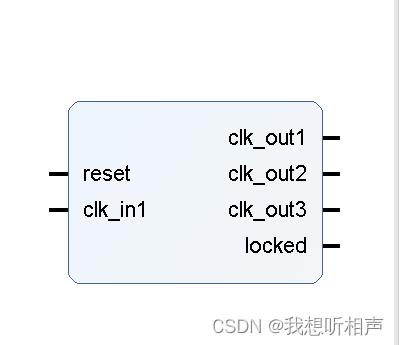
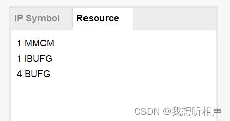
个人经验:如工程设计中使用局时钟树资源,一般使用clocking wizard IP和更为方便,该IP和包含了MMCM+IBUFG+BUFG,,如下图一个单端系统输入时钟+三个输出时钟的WIZ IP核所示:
2、IBUFG+DCM+BUFG
首先通过DCM数字锁相环适用于动态调整,然后再通过BUFG利用全局时钟树走线。
3、logic+BUFG
FPGA内部的普通logic信号也可以通过通过BUFG利用全局时钟树走线,需要注意的是logic到BUFG之间大概有10ns的延时。
4、logic+DCM+BUFG
FPGA内部的普通logic信号也可以首先通过DCM数字锁相环调整,然后再通过BUFG利用全局时钟树走线。
5、IBUFGDS+BUFG
差分时钟信号的组合使用方法。
一般使用是同1.所述常用clocking wizard IP得到工程所需的各速率的时钟信号,该IP核的输入可选择为差分输入时钟。
6、IBUFDS+BUFG
差分普通信号作为全局时钟信号的的组合使用方法。
二、普通IO输出时钟信号时的推荐方法
若直接使用assign 将clk_object(BUFG输出信号)赋值给IO管脚作为输出,
推荐使用原语ODDR作为实现,代码如下:
- ODDR #(
- .DDR_CLK_EDGE("OPPOSITE_EDGE"), // "OPPOSITE_EDGE" or "SAME_EDGE"
- .INIT(1'b0), // Initial value of Q: 1'b0 or 1'b1
- .SRTYPE("SYNC") // Set/Reset type: "SYNC" or "ASYNC"
- ) ODDR_inst1 (
- .Q(实际作为时钟输出信号的IO管脚), // 1-bit DDR output
- .C(本计划作为输出的时钟信号), // 1-bit clock input
- .CE(1'b1), // 1-bit clock enable input
- .D1(1'b1), // 1-bit data input (positive edge)
- .D2(1'b0), // 1-bit data input (negative edge)
- .R(1'b0), // 1-bit reset
- .S(1'b0) // 1-bit set
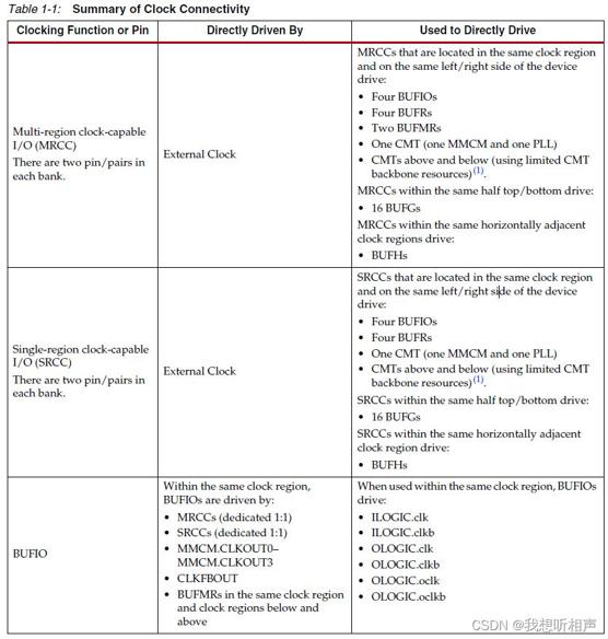
UG472中P24对BUFIO的描述:
The main purpose of the BUFR and BUFIO combination is to support source-synchronous
interfaces. When an interface is placed into a single region, the BUFIO clocks the
high-speed side of the SelectIOs and the BUFR clocks the deserialized/serialized side at a
lower speed into the FPGA logic providing the clock domain transfer function. For
interfaces that require more logic and/or I/Os than are available in a single clock region/
bank, the BUFMR (BUFMRCE) is used to expand clock domain transfer functionality into
the clock regions above and below. Certain types of applications that require a divided
clock not related to the source-synchronous I/O use case can use a BUFR as a simple clock
divider when an MMCM/PLL cannot be used or is not available for the frequency divide
function. In this case, particular attention must be paid to the timing and skew because this
is not the primary purpose of the BUFR. For more information on clocking SelectIO
resources, consult UG471, 7 Series FPGAs SelectIO Resources User Guide.
BUFIO的输入输出YG472中描述如下:(因此BUFIO的输出可以驱动SELECTIO的I/OLOGIC)
Within the same clock region, BUFIOs are driven by:
• MRCCs (dedicated 1:1)
• SRCCs (dedicated 1:1)
• MMCM.CLKOUT0– MMCM.CLKOUT3
• CLKFBOUT
• BUFMRs in the same clock region and clock regions below and above
When used within the same clock region, BUFIOs drive:
• ILOGIC.clk
• ILOGIC.clkb
• OLOGIC.clk
• OLOGIC.clkb
• OLOGIC.oclk
• OLOGIC.oclkb
评论记录:
回复评论: